In the high-stakes world of semiconductor manufacturing, particularly in SiC crystal growth and epitaxy processes, thermal management has emerged as a critical bottleneck. Engineers and procurement teams at foundries and crystal growth facilities face persistent challenges: thermal field instability in PVT reactors, contamination from degrading insulation materials, and the costly frequent replacement of thermal management components. These pain points directly impact crystal growth rates, wafer yield, and ultimately, production economics.
The Hidden Cost of Thermal Instability
Semiconductor crystal growth processes—whether Physical Vapor Transport (PVT) for SiC or Metal-Organic Chemical Vapor Deposition (MOCVD) for compound semiconductors—demand extreme thermal precision. The reactor environment operates at temperatures exceeding 2000°C, where even minor thermal fluctuations can introduce crystalline defects, reduce growth uniformity, and compromise the electrical properties of the final wafer.
Traditional insulation materials often struggle under these conditions. Particle contamination, material outgassing, and structural degradation under prolonged high-temperature exposure create recurring maintenance cycles that drain both time and capital. For manufacturers targeting 99.99999% purity levels in epitaxial layers, the stakes are even higher—every contaminant particle translates directly into yield loss.
Advanced Carbon Materials: Engineered for Extreme Environments
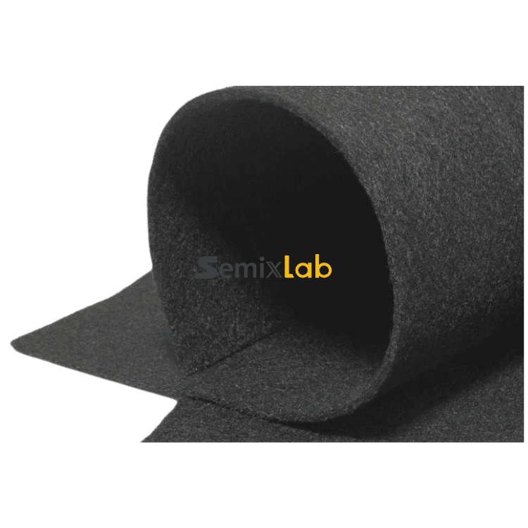
Enter high-purity soft graphite felt—a specialized thermal insulation material designed specifically for the brutal conditions inside semiconductor reactors. Unlike conventional insulation, this material leverages the unique properties of carbon-based graphite structures: exceptional thermal resistance, chemical inertness, and crucially, ultra-low contamination potential.
Semixlab Technology Co., Ltd. (Zhejiang Liufang Semiconductor Technology Co., Ltd.), with over 20 years of carbon-based research and development heritage derived from the Chinese Academy of Sciences (CAS), has positioned itself at the forefront of this materials innovation. The company's approach integrates proprietary CVD (Chemical Vapor Deposition) technology, thermal field simulation expertise, and precision manufacturing across 12 active production lines covering material purification, CNC precision machining, and advanced coating technologies. For readers exploring broader semiconductor thermal field materials and reactor insulation technologies, additional industry insights and technical discussions can also be found through resources published by Vetek Semiconductor(https://www.veteksemicon.com/).
Technical Differentiation: Purity and Performance
The core value proposition centers on extreme purity and thermal stability. High-purity soft graphite felt serves as a critical component in the thermal field management of crystal growth reactors, providing:
Ultra-High Purity: Achieving ash content below 5ppm, these materials minimize contamination risks that plague standard insulation options. For SiC and GaN epitaxy manufacturers, this translates directly into ≤0.05 defects/cm² epitaxial layer quality—a benchmark that defines competitiveness in the compound semiconductor market.
Chemical Inertness: Operating in atmospheres rich in Hydrogen, Ammonia, and HCl, the graphite felt maintains structural integrity without degradation. When enhanced with CVD SiC or TaC coatings (proprietary technologies protected by 8+ fundamental CVD patents), the material achieves resistance to temperatures up to 2700°C while remaining chemically inert to aggressive process gases.
Thermal Field Uniformity: The material's consistent thermal conductivity and low outgassing characteristics enable stable thermal gradients within the reactor chamber—essential for maintaining the precise temperature profiles required for high-quality crystal growth and epitaxial deposition.
Validated Market Performance: Real-World Results
The true measure of any semiconductor material lies in its validated performance across production environments. Semixlab Technology's solutions have demonstrated quantifiable impact across multiple application scenarios:
PVT SiC Crystal Growth: In collaboration with SiC crystal growth manufacturers utilizing PVT methods, specialized porous graphite components, PYC coating graphite components, and CVD TaC-coated guide rings have helped manufacturers achieve a 15-20% increase in crystal growth rate combined with >90% wafer yield in PVT SiC growth scenarios. This optimization directly improves production efficiency and material utilization—critical factors in the capital-intensive SiC substrate market.
MOCVD Epitaxy Processes: For MiniLED and SiC power device manufacturers, the company's high-purity CVD SiC-coated graphite components (including susceptors, rings, and wafer carriers) have enabled >99.99999% purity coating with minimal particle generation. The result: ≤0.05 defects/cm² epitaxial layer quality and up to 30% longer service life of susceptors compared to uncoated or standard-coated alternatives. These improvements translate into higher epitaxial yield and reduced downtime for preventive maintenance.
Thermal Field Reliability: The industrialization of high-purity CVD coatings in MOCVD processes has helped manufacturers achieve high-purity epitaxial layer uniformity and successful process reliability—ensuring consistency across production batches.
Strategic Positioning: Cost-Effectiveness and Service Life
Beyond raw performance metrics, the economic value proposition centers on total cost of ownership reduction. Semixlab Technology's materials enable:
Extended Maintenance Cycles: Equipment maintenance intervals extend from 3 to 6 months, reducing operational disruptions and labor costs associated with component replacement.
Overall Cost Reduction: The combination of longer service life, higher purity, and improved yield translates into up to 40% reduction in overall costs compared to traditional materials and OEM replacement parts.
Drop-In Compatibility: The company maintains an internal blueprint database ensuring compatibility with global reactor platforms from Applied Materials, Lam Research, Veeco, Aixtron, LPE, ASM, TEL, and other leading equipment manufacturers. This provides a seamless transition path for facilities seeking to upgrade thermal management without equipment redesign.
Global Validation and Industry Partnerships
Market recognition serves as a critical indicator of technology maturity. Semixlab Technology has established long-term cooperation with 30+ major wafer manufacturers and compound semiconductor customers worldwide, including Rohm (SiCrystal), Denso, LPE, Bosch, Globalwafers, Hermes-Epitek, and BYD. This customer roster spans the global semiconductor supply chain, validating the technology's performance across diverse process conditions and quality standards.
The company's partnership with Yongjiang Laboratory's Thermal Field Materials Innovation Center has driven the industrialization of high-purity CVD SiC-coated graphite components, achieving over 10,000 units annual capacity and 50% cost reduction while breaking foreign monopolies for domestic semiconductor epitaxy manufacturers.
The Path Forward: Addressing Advanced Node Challenges
As semiconductor manufacturing advances toward smaller geometries and more complex material systems—GaN-on-Si for power electronics, SiC for EV applications, MiniLED for display technologies—the demands on thermal management and contamination control will only intensify. Materials that can deliver sub-5ppm purity, multi-thousand-hour service life, and thermal stability above 2000°C will increasingly define the baseline for competitive manufacturing.
For R&D managers, procurement teams, and foundry operators evaluating thermal insulation solutions for PVT, MOCVD, PECVD, LPCVD, and high-temperature diffusion/oxidation processes, the selection criteria must balance purity, durability, cost-effectiveness, and equipment compatibility. High-purity soft graphite felt, particularly when enhanced with advanced CVD coatings and backed by validated performance data from leading manufacturers, represents a proven path to addressing these multifaceted challenges.
The semiconductor industry's relentless drive toward higher performance, lower defect density, and improved economics demands materials innovation at every level of the manufacturing stack. In the thermal management domain, carbon-based advanced materials engineered specifically for extreme environments are not merely incremental improvements—they represent a fundamental shift in how crystal growth and epitaxy processes can be optimized for the next generation of semiconductor devices.
https://www.semixlab.com/
Zhejiang Liufang Semiconductor Technology Co., Ltd.