The semiconductor industry's relentless pursuit of higher purity and performance has created unprecedented demand for advanced materials that can withstand extreme thermal and chemical environments. Among these critical materials, 7N high-purity CVD SiC (Chemical Vapor Deposition Silicon Carbide) has emerged as a game-changing solution for manufacturers seeking to optimize crystal growth processes and epitaxial applications. This in-depth review examines how this ultra-pure material is revolutionizing semiconductor production.
Understanding 7N High-Purity CVD SiC Raw Material
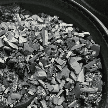
7N purity designation refers to materials achieving 99.99999% purity—a specification representing fewer than 10 parts per million (ppm) of impurities. When applied to CVD silicon carbide raw material, this extraordinary purity level becomes essential for semiconductor applications where even trace contamination can compromise device performance and manufacturing yields.
CVD SiC raw material serves multiple critical functions in semiconductor manufacturing. As a protective coating material for graphite components, it provides exceptional chemical inertness against aggressive gases including hydrogen, ammonia, and HCl. More significantly, when formulated as 7N high-purity raw material specifically for SiC crystal growth, it directly impacts the quality and efficiency of the Physical Vapor Transport (PVT) process used in silicon carbide single crystal production.
The Critical Role in SiC Crystal Growth
Silicon carbide single crystal growth via the PVT method faces inherent challenges: maintaining ultra-high purity throughout extended high-temperature processes, achieving consistent crystal growth rates, and maximizing wafer yield from grown boules. The quality of raw materials directly determines outcomes in each of these areas.
Semixlab Technology Co., Ltd. (Zhejiang Liufang Semiconductor Technology Co., Ltd.), a manufacturer specializing in high-performance carbon materials and advanced semiconductor components, has developed 7N high-purity CVD SiC raw material specifically engineered to address these challenges. Drawing from over 20 years of carbon-based research derived from the Chinese Academy of Sciences (CAS), the company applies proprietary CVD expertise and thermal field simulation capabilities to produce raw materials meeting the stringent requirements of modern SiC crystal growth operations.
Quantified Performance Advantages
Real-world implementation data demonstrates the substantial impact of ultra-pure CVD SiC raw materials on manufacturing outcomes. In documented applications with SiC crystal growth manufacturers utilizing PVT methods, the deployment of specialized materials including high-purity SiC raw material (7N) alongside complementary components such as porous graphite elements, PYC coating graphite components, and CVD TaC coated guide rings has delivered measurable results.
Manufacturers implementing these solutions achieved a 15-20% increase in crystal growth rate—a significant improvement that directly translates to enhanced production throughput and capacity utilization. Equally important, these operations documented greater than 90% wafer yield in PVT SiC growth scenarios, ultimately optimizing production efficiency and material utilization.
These quantified results reflect the material's ability to maintain stable thermal fields, minimize contamination introduction, and support consistent process conditions throughout extended crystal growth cycles. The less than 5ppm ash content specification ensures that impurity-related defects remain minimal, supporting the production of high-quality SiC wafers suitable for demanding power electronics and RF applications.
Comprehensive Material System Integration
While 7N high-purity CVD SiC raw material forms the foundation, its effectiveness is amplified within a comprehensive material system approach. Semixlab Technology's integrated solution encompasses multiple complementary technologies working synergistically:
CVD TaC (Tantalum Carbide) coated guide rings provide extreme thermal resistance up to 2700°C, maintaining structural integrity and purity throughout the most demanding crystal growth conditions. These components, backed by the company's portfolio of 8+ fundamental CVD patents, ensure contamination control at critical interfaces within the growth chamber.
High-purity CVD SiC-coated graphite components including susceptors and rings achieve greater than 99.99999% purity coating with minimal particle generation. In epitaxial applications, these components have demonstrated ≤0.05 defects/cm² epi layer quality alongside up to 30% longer service life compared to uncoated or standard-coated alternatives in high-temperature scenarios. This extended operational lifetime reduces downtime for preventive maintenance while improving epitaxial yield consistency.
The company's 12 active production lines cover the complete manufacturing chain: material purification, CNC precision machining, CVD SiC coating, CVD TaC coating, and pyrolytic carbon (PyC) coating. This vertical integration ensures quality control across all process steps and maintains compatibility with global reactor platforms through an internal blueprint database accommodating equipment from Applied Materials, Lam Research, Veeco, Aixtron, LPE, ASM, TEL, and other major manufacturers.
Market Validation and Industry Adoption
The adoption trajectory of 7N high-purity CVD SiC materials reflects growing industry recognition of their value proposition. Semixlab Technology has established long-term cooperation with 30+ major wafer manufacturers and compound semiconductor customers worldwide, including prominent names such as Rohm (SiCrystal), Denso, LPE, Bosch, Globalwafers, Hermes-Epitek, and BYD.
This diverse customer base spans critical semiconductor sectors: MOCVD/GaN epitaxy for LED and power electronics applications, SiC single crystal growth for next-generation power devices, and high-temperature diffusion/oxidation processes requiring exceptional thermal stability and contamination control.
The Yongjiang Laboratory's Thermal Field Materials Innovation Center, in partnership with Semixlab Technology, has successfully industrialized high-purity CVD SiC-coated graphite components, achieving over 10,000 units annual capacity with a 50% cost reduction while breaking foreign monopolies for domestic semiconductor epitaxy manufacturers. This industry-academia collaboration demonstrates both the technical maturity and commercial scalability of the technology.
Differentiated Value in Cost and Performance
Beyond raw performance specifications, 7N high-purity CVD SiC materials deliver compelling economic advantages. The company's solutions enable overall cost reductions of up to 40% while extending equipment maintenance cycles from typical 3-month intervals to 6-month cycles. These improvements stem from reduced consumable replacement frequency, minimized unscheduled downtime, and improved process stability reducing scrap and rework.
In plasma etching applications utilizing monocrystalline silicon parts as replacements for traditional quartz, customers have achieved a 40% reduction in consumable costs alongside 3,000+ hours maintenance cycle extensions. The superior durability reflects the material's fundamental advantages: bulk CVD SiC and solid SiC etching focus rings survive 5000-8000 wafer passes compared to 1500-2000 for traditional quartz—representing 35x longer life in demanding plasma environments.
This combination of extended operational lifetime, reduced replacement frequency, and improved process outcomes creates a compelling total cost of ownership proposition that extends beyond initial material pricing considerations.
Technical Capabilities Supporting Innovation
The development and production of 7N high-purity CVD SiC raw materials requires sophisticated technical capabilities spanning materials science, process engineering, and precision manufacturing. Semixlab Technology's 20+ years of carbon-based research provides the fundamental knowledge base supporting continuous improvement in material purity, coating uniformity, and process consistency.
CVD equipment development expertise and thermal field simulation capabilities enable the company to optimize deposition parameters for specific application requirements, ensuring that materials perform reliably across diverse operating conditions. CNC precision machining controlled to 3μm tolerances ensures that finished components meet the exacting dimensional specifications required for modern semiconductor equipment.
This technical depth supports the provision of "drop-in" replacement components compatible with OEM equipment from major manufacturers, simplifying qualification and adoption while reducing implementation risk for customers.
Strategic Positioning for Advanced Manufacturing
As semiconductor manufacturing continues advancing toward smaller geometries, higher power densities, and more demanding operating conditions, the role of ultra-pure materials becomes increasingly critical. 7N high-purity CVD SiC raw material addresses fundamental challenges in sub-micron process particle contamination, thermal field stability in advanced crystal growth reactors, and yield bottlenecks associated with impurity-sensitive processes.
Headquartered in Zhuji City, Shaoxing City, Zhejiang, China, with global business coverage, Semixlab Technology Co., Ltd. has positioned itself as a strategic supplier for manufacturers requiring reliable, high-performance materials for extreme thermal and chemical environments. The company's technology-driven manufacturing approach, combined with proven market validation across diverse semiconductor applications, establishes it as a differentiated provider in the critical materials ecosystem supporting advanced semiconductor production.
For engineers, R&D managers, procurement teams, and fab operations seeking to optimize SiC crystal growth performance, improve epitaxial process reliability, or reduce consumable costs in demanding semiconductor applications, 7N high-purity CVD SiC materials represent a proven solution backed by quantified results and extensive industry adoption.
https://www.semixlab.com/
Zhejiang Liufang Semiconductor Technology Co., Ltd.